 |
JTAG, an acronym for Joint Test Action Group, is the usual name used for the IEEE 1149.1 standard entitled Standard Test Access Port and Boundary-Scan Architecture for test access ports used for testing printed circuit boards using boundary scan.
JTAG was standardized in 1990 as the IEEE Std. 1149.1-1990. In 1994, a supplement that contains a description of the boundary scan description language (BSDL) was added. Since then, this standard has been adopted by electronics companies all over the world. Boundary-scan is nowadays mostly synonymous with JTAG.
While designed for printed circuit boards, it is nowadays primarily used for testing sub-blocks of integrated circuits, and is also useful as a mechanism for debugging embedded systems, providing a convenient "back door" into the system. When used as a debugging tool, an in-circuit emulator which in turn uses JTAG as the transport mechanism enables a programmer to access an on-chip debug module which is integrated into the CPU via JTAG. The debug module enables the programmer to debug the software of an embedded system.
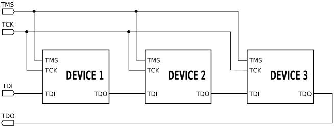
A JTAG interface is a special four/five-pin interface added to a chip, designed so that multiple chips on a board can have their JTAG lines daisy-chained together, and a test probe need only connect to a single "JTAG port" to have access to all chips on a circuit board. The connector pins are
|
Since only the one data line is available, the protocol is necessarily serial like SPI. The clock input is at the TCK pin. Configuration is performed by manipulating a state machine one bit at a time through a TMS pin. One bit of data is transferred in and out per TCK clock pulse at the TDI and TDO pins, respectively. Different instruction modes can be loaded to read the chip ID, sample input pins, drive (or float) output pins, manipulate chip functions, or bypass (pipe TDI to TDO to logically shorten chains of multiple chips). The operating frequency of TCK varies depending on the chip, but it is typically 10-100 MHz (10-100ns per bit).
When performing boundary scan on integrated circuits, the signals manipulated are between different functional blocks of the chip, rather than between different chips.
The TRST pin is an optional active-low reset to the test logic - usually asynchronous, but sometimes synchronous, depending on the chip. If the pin is not available, the test logic can be reset by clocking in a reset instruction synchronously.
Even though few consumer products provide an explicit JTAG port connector, the connections are very often available on the printed circuit board as a remnant from development prototyping. When exploited, these connections often provide an excellent means for reverse engineering.